In the semiconductor field, material performance often determines the power limits, reliability lifespan, and packaging efficiency of products. As chip sizes continue to shrink and power densities continue to rise, traditional pure copper and pure tungsten materials are gradually exposing their limitations, such as insufficient heat dissipation speed, excessive thermal expansion coefficient mismatch, susceptibility to hot spots, or failure due to thermal fatigue. In this context, nano tungsten-copper composite materials, with high thermal conductivity, adjustable thermal expansion coefficient, and excellent mechanical properties, are becoming an important new material direction in high-end semiconductor manufacturing. Compared to traditional tungsten-copper, the greatest value of nano tungsten-copper lies in its smaller structural scale, stronger interface bonding, and faster thermal diffusion speed, which can significantly enhance heat dissipation efficiency and extend product lifespan. Many highly temperature-sensitive thermal management components in semiconductor manufacturing, such as power device heat sinks, laser heat dissipation bases, and chip packaging back metals, have begun to try replacing traditional materials with nano tungsten-copper to achieve more stable system performance with greater engineering safety margins.
1.Role Mechanism of Nano Tungsten-Copper in the Semiconductor Field
The reason nano tungsten-copper is favored in the semiconductor industry lies in the multiple performance advantages brought by its microscopic structure:
Nano interfaces promote rapid thermal diffusion Nano-scale interfaces make heat flow transfer smoother within the material, less likely to cause local hot spots due to interface thermal resistance. This advantage is particularly prominent in chip backside heat dissipation (BGBM) structures, helping to reduce chip operating temperature.
Better thermal expansion matching with semiconductor materials The thermal expansion coefficient of nano tungsten-copper can be adjusted over a wide range, making it more compatible with materials such as Si, GaN, and GaAs, effectively reducing stress generated during thermal cycling and improving solder joint reliability.
High hardness and high uniformity improve micro-machining performance In precision molds, electrodes, and micro-structure processing, the nano structure provides better dimensional stability, less prone to deformation or tool marks during processing, thus achieving higher surface quality. These mechanisms work together to give nano tungsten-copper obvious advantages in high-power, high-frequency, and high-reliability semiconductor devices.
2.Industrial Significance of Nano Tungsten-Copper in the Semiconductor Field
As technology advances from traditional ICs to high-power scenarios such as AI accelerators, automotive power modules, and 5G RF front-ends, the entire industry faces a common challenge: heat has become the primary bottleneck affecting chip performance and lifespan. Nano tungsten-copper materials, due to their superior thermal conductivity and structural designability, are considered an important path to solve this bottleneck: (1) can improve heat dissipation efficiency of high-power devices, thereby supporting higher operating currents and frequencies; (2) can reduce stress in packaging structures caused by thermal expansion mismatch, improving long-term device reliability; (3) can be used in laser devices, radar, fast-charging modules, and other applications extremely sensitive to temperature; (4) can meet the substantial demand for enhanced heat dissipation capability in future smart vehicles, AI chips, and ultra-large-scale packaging (SiP/3D IC). Therefore, nano tungsten-copper is not only a material upgrade but also represents a system-level evolution direction for semiconductor heat dissipation technology.
3.Main Application Directions of Nano Tungsten-Copper in the Semiconductor Field
High-power chip heat dissipation substrates (IGBT, MOSFET, GaN/SiC power devices) These devices generate extremely high heat flux density during operation. Nano tungsten-copper has the advantages of high thermal conductivity and controllable thermal expansion, which can significantly reduce temperature fluctuations on the chip backside, reduce solder joint fatigue cracks, and improve overall lifespan.
Packaging heat spreaders and heat diffusion plates (Heat Spreader / Heat Sink) In CPU, GPU, AI accelerators, and various server chips, nano tungsten-copper is used as a high-end heat spreader material. Due to its more stable thermal diffusion capability and less prone to hot spots, it helps stabilize the operating temperature of high-computing-power chips
Heat dissipation bases for high-power lasers and RF power modules Laser chips and RF power devices are extremely sensitive to temperature; slight fluctuations can affect output accuracy or even damage the device. Nano tungsten-copper is one of the preferred materials due to its low thermal resistance, fast thermal diffusion, and high dimensional stability.
Electrodes/target materials in electron beam equipment and ion implantation equipment Such equipment undertakes key tasks on semiconductor production lines, with high operating environment temperatures and large impacts. The high wear resistance, high-temperature stability, and long lifespan of nano tungsten-copper can significantly reduce equipment downtime maintenance costs.
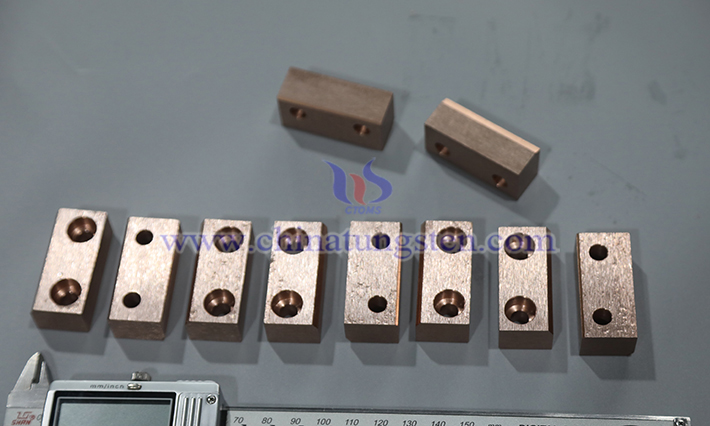
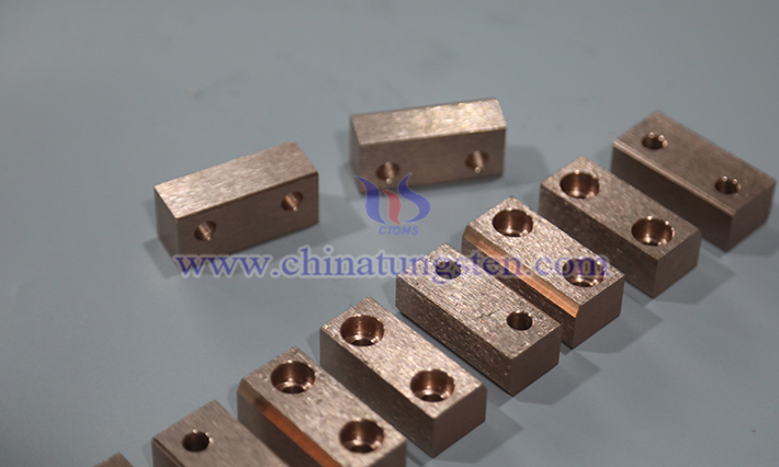
EDM precision electrodes in semiconductor manufacturing Many precision molds, communication devices, or micro-cavities require EDM discharge processing. Nano tungsten-copper electrodes have wear resistance and uniform discharge, enabling higher processing precision and less electrode consumption.


